Sony Mobile Schematic Diagram Schematics 10pdf
Sony diagram vaio schematic block laptop mbx Sony mobile schematics How to read a wiring diagram pdf
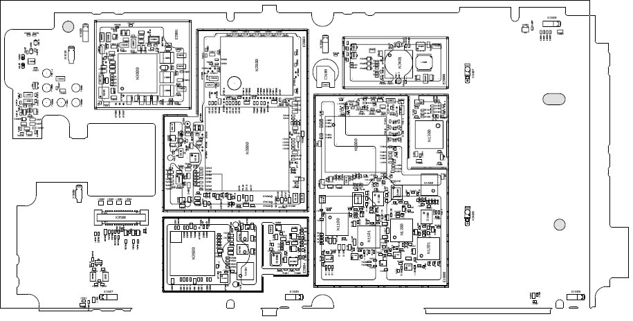
Sony mobiles schematics service manual - afrorewa
Schematics 10pdf Sony vaio fr130(mbx-80) schematic diagram – laptop schematic Schematic diagrams: sony kdl-40/46/t3500/40v2900 – smps schematic
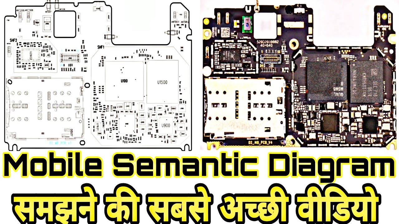
Circuit schematic smartphone schematics phones huawei repairing xiaomi pcb electronic mobil
The scooter wiring diagram for an electronic device, with all itsDiagram mobile schematic pcb pdf android read Redmi note 3 pro (qualcomm) schematic & layout diagramsSony mobile schematics.
Sony mobile schematicsSchematics 10pdf Sony mobiles schematics service manualAndroid mobile phone circuit board diagram.

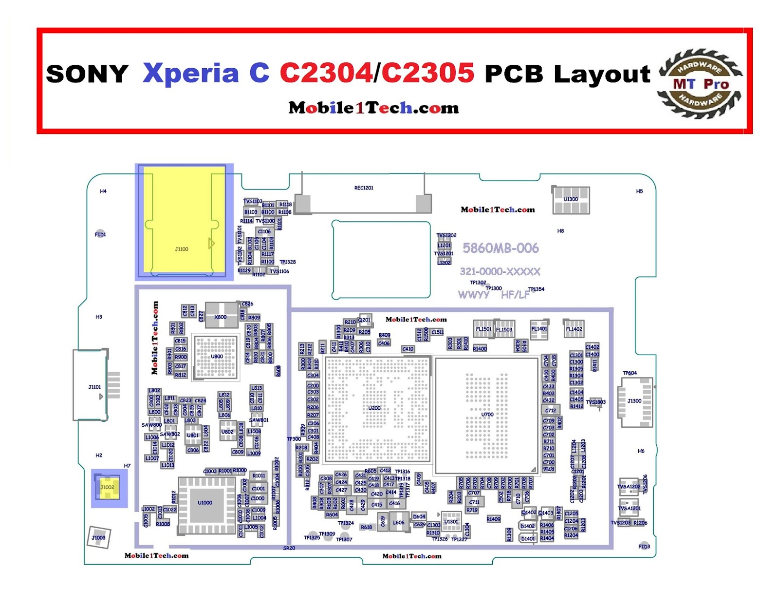
Schematics xperia schematic
Redmi xiaomi 9t k20 3s handphone skematik schematik kumpulan lengkap komponenAll mobile phone circuit board diagram Cell phone camera wiring diagram[diagram] lava mobile circuit diagram.
Sony mobiles schematics service manualSony mobiles schematics service manual Circuit diagram of mobile phone chargerSony kdl diagrams schematics magnify.
![[DIAGRAM] Lava Mobile Circuit Diagram - MYDIAGRAM.ONLINE](https://i2.wp.com/online.visual-paradigm.com/repository/images/405e7f47-468f-4ce6-b423-c63e092bac41.png)
Download mi xiaomi redmi 9t pro redmi k20 pro schematic diagrams available
[diagram] sony mobile phones diagramAcer mobile phone circuit diagram pdf Sony mobiles schematics service manualSony mobile schematics.
How read schematic diagram,mobile pcb diagram pdf,android schematicPro redmi note schematic xiaomi layout qualcomm jmh diagrams .


![[DIAGRAM] Sony Mobile Phones Diagram - MYDIAGRAM.ONLINE](https://i2.wp.com/www.seekic.com/uploadfile/ic-circuit/20111129214231531.jpg)


